Over the past few years, there has been a lot of talk about standardization on a single core platform to simplify the migration of designs from one MCU vendor to another.
The interesting thing is, in all of this talk there is no mention of the peripherals. But peripherals are at the heart of what it really takes to port an application from one MCU vendor to another.
It’s all about the peripherals
When an engineer starts a new design, he will begin by looking at its functional requirements. What is the system supposed to do? How does the user interact with it? So on and so forth.
Based on this, he will determine the circuitry needed and the on-chip MCU peripherals that are required to control these circuits. For example, an industrial HMI (Human Machine Interface) device will need to support a LCD, buttons and/or a touch screen, communication to the machine, LEDs, a speaker/buzzer, etc.
All of these functions will require some kind of peripheral on the MCU, e.g., a CAN controller for communication, an ADC for a touch screen, a PWM timer for a buzzer, etc.
The more functionality a peripheral has, the less external circuitry is needed, which, in some cases, reduces the amount of code that needs to be written. For example, utilizing a special buzzer mode is easier than having to set up a PWM for the same purpose.
The core requirements are usually straightforward. While very important, the designer is quite abstracted from the core itself. The core really must meet two basic criteria.
Is it fast enough to perform all of the software tasks that are required to create the best user experience? And, does it perform all of these tasks efficiently? The type of core is irrelevant beyond this, as long as it meets these two performance requirements.
Of course, there is also a firmware/software side to the core. Legacy code is something the engineer has to consider. How much work can he save by using existing code? This question is not linked to the core directly, but rather to the peripherals, as most 32-bit MCU code is written in C and as such can be recompiled to any core.
Each MCU manufacturer will have peripheral features and programming models that are unique to its own products, regardless of the core that is being employed, which is what really makes the code hard to port.
Firmware libraries
To help the engineer, each MCU manufacturer supplies a firmware library that contains code to set up and use the various on-chip MCU peripherals. Because these peripherals are implemented in different ways by each manufacturer, and even have different features, porting an application from one MCU to another is not trivial.
ARM has been trying to ease porting efforts by defining a firmware abstraction layer standard called the Cortex Microcontroller Software Interface Standard (CMSIS), and the MCU manufacturers that use the Cortex-M series of cores have adopted it in their firmware libraries.
Unfortunately, this standard does not address the difficulty of porting peripherals, nor does it have a standard naming convention on variables or functions. As a result, there is no easy way to move from one firmware library to another without significant work.
In fact, this standard makes almost no improvement in the effort it takes to port an application among ARM MCU vendors. After all, there is no benefit to the MCU manufacturers in making it too easy to move to another vendor’s product.
Design for portability
Since the MCU manufacturer will not simplify portability to another vendor’s product, it is up to the design engineer to make the design portable. This can be achieved by implementing an abstraction layer that creates a standard programming interface between the hardware (i.e., MCU peripherals) and the application code. There are at least two ways to approach this:
1) Develop a shim layer or wrapper to translate between the MCU manufacturer’s peripheral library and your code. This is probably the most time-efficient solution, but it will add more code in the command and data paths.
2) Define a standard function and variable naming scheme, and apply it to each peripheral library. This avoids adding code, but can be very time consuming, depending on how complex your peripheral usage is.
Portability is not trivial and has to be part of the development process from day one. On top of the firmware/software side, there is the question of pin-to-pin compatibility, which almost always means re-layout of the PCB when moving from one MCU vendor to another. And, there might also be requirements for different external parts, such as capacitors and regulators.
Bottom line
Portability between 32-bit MCU vendors is equally difficult, regardless of the core being used. It is all about the peripherals and related firmware libraries. Each MCU manufacturer will do his best to make the design process as easy as possible by supplying firmware libraries and application notes.
They will also try to make their parts such that you can move between their own families with minimal effort. But portability to a competing solution is something they will not be interested in making too simple.
This is something the design engineer will have to own, and thus should evaluate the cost/benefits of doing so at the beginning of each project.
Information is shared by www.irvs.info
Friday, April 29, 2011
Tuesday, April 26, 2011
Architecting the smart grid for security
The smart grid is an important, emerging source of embedded systems with critical security requirements. One obvious concern is financial: for example, attackers could manipulate metering information and subvert control commands to redirect consumer power rebates to false accounts. However, smart grids imply the addition of remote connectivity, from millions of homes, to the back end systems that control power generation and distribution. The ability to impact power distribution has obvious safety ramifications, and the potential to impact a large population increases the attractiveness of the target.
These back end systems are protected by the same security technologies (firewalls, network access authentication, intrusion detection and protection systems) that today defend banks and governments against Internet-borne attacks. Successful intrusions into these systems are a daily occurrence. The smart grid, if not architected properly for security, may provide hostile nation states and cyber terrorists with an attack path from the comfort of their living rooms. Every embedded system on this path – from the smart appliance to the smart meter to the network concentrators – must be secure.
The good news is that utilities and their suppliers are still early in the development of security strategy and network architectures for smart grids; a golden opportunity now exists to build security in from the start.
Sophisticated attackers
The increasing reliance of embedded systems in commerce, critical infrastructure, and life-critical function makes them attractive to attackers. Embedded industrial control systems managing nuclear reactors, oil refineries, and other critical infrastructure present opportunity for widespread damage. To get an idea of the kinds of sophisticated attacks we can expect on the smart grid, look no further than the recent Stuxnet attack on nuclear power infrastructure.
Stuxnet infiltrated Siemens process control systems at nuclear power plants by first subverting the Microsoft Windows workstations operators use to configure and monitor the embedded control electronics (Figure 1). The Stuxnet worm is likely the first malware to directly target embedded process control systems and illustrates the incredible damage potential in modern smart grid security attacks.

Figure 1 - Stuxnet infiltration of critical power control system via operator PC
information is shared by www.irvs.info
Monday, April 25, 2011
Facilitating at-speed test at RTL
Production testing for complex chips usually involves multiple test methods. Scan-based automatic test pattern generation (ATPG) for the stuck-at defect model has been the standard for many years, but experience as well as a number of theoretical analyses have shown that the stuck-at fault model is incomplete. Many devices pass high coverage stuck-at tests and still fail to operate in system mode.
Analysis of the defective chips often reveals that speed or timing problems are the culprits. At 90nm and smaller processes, the percentage of timing related defects is so high that static testing is no longer considered sufficient. Functional tests have been used to check (cheque for banks) for at-speed operation. But generating functional at-speed test patterns is difficult and running this volume of tests on the automatic test equipment (ATE) is expensive. As an alternative, scan test has been adapted to detect timing-related defects. Like standard stuck-at scan tests, high coverage at-speed scan test vectors can be automatically generated by ATPG tools. Manufacturing testing of deep subµm designs now routinely includes "at-speed" tests along with stuck-at tests.
Little has been done so far to make front end designers aware of at-speed test solutions at the register transfer language (RTL) level of abstraction. This document is intended to present basic concepts and issues for at-speed testing, as well as demonstrate the at-speed coverage estimation and diagnosis capability built-in to the SpyGlass-DFT DSM product for RTL designers and test engineers.
Information is shared by www.irvs.info
Tuesday, April 19, 2011
Mobile WiMAX system operation
This chapter provides a detailed description of the operation of IEEE 802.16m entities (i.e., mobile station, base station, femto base station, and relay station) through use of state diagrams and call flows. An attempt has been made to characterize the behavior of IEEE 802.16m systems in various operating conditions such as system entry/re-entry, cell selection/reselection, intra/inter-radio access network handover, power management, and inactivity intervals.
This chapter describes how the IEEE 802.16m system entities operate and what procedures or protocols are involved, without going through the implementation details of each function or protocol. The detailed algorithmic description of each function and protocol will be provided in following chapters. Several scattered call flows and state diagrams were used in reference [1] to demonstrate the behavior of the legacy mobile and base stations, making it difficult to coherently understand the system behavior.
The IEEE 802.16 standards have not generally been developed with a system-minded view; rather, they specify components and building blocks that can be integrated to build a working and performing system. An example is the mobile WiMAX profiles where a specific set of IEEE 802.16-2009 standard features (one out of many possible configurations) were selected to form a mobile broadband wireless access system.
Detailed IEEE 802.16m entities' state transition diagrams comprising states, constituent functions, and protocols within each state, and inter-state transition paths conditioned to certain events would help the understanding and implementation of the standards specification [2–5]. It further helps to understand the behavior of the system without struggling with the distracting details of each constituent function.
State diagrams are used to describe the behavior of a system. They can describe possible states of a system and transitions between them as certain events occur. The system described by a state diagram must be composed of a finite number of states. However, in some cases, the state diagram may represent a reasonable abstraction of the system.
There are many forms of state diagrams which differ slightly and have different semantics. State diagrams can be used to graphically represent finite state machines (i.e., a model of behavior composed of a finite number of states, transitions between those states, and actions). A state is defined as a finite set of procedures or functions that are executed in a unique order. In the state diagram, each state may have some inputs and outputs, where deterministic transitions to other states or the same state happen based on certain conditions.
In this chapter, the notion of mode is used to describe a sub-state or a collection of procedures/protocols that are associated with a certain state. The unique definition of states and their corresponding modes and protocols, and internal and external transitions, is imperative to the unambiguous behavior of the system. Also, it is important to show the reaction of the system to an unsuccessful execution of a certain procedure. The state diagrams described in the succeeding sections are used to characterize the behavior of IEEE 802.16m system entities.
This chapter provides a top-down systematic description of IEEE 802.16m entities' state transition models and corresponding procedures, starting at the most general level and working toward the details or specifics of the protocols and transition paths. An overview of 3GPP LTE/LTE-Advanced states and user equipment state transitions is further provided to enable readers to contrast the corresponding terminal and base station behaviors, protocols, and functionalities. Such contrast is crucial in the design of inter-system interworking functions.
information is shared by www.irvs.info
Friday, October 8, 2010
Digital Electronics
Introduction
The first single chip microprocessor came in 1971 by Intel Corporation. It was called Intel 4004 and that was the first single chip CPU ever built. We can say that was the first general purpose processor. Now the term microprocessor and processor are synonymous. The 4004 was a 4-bit processor, capable of addressing 1K data memory and 4K program memory. It was meant to be used for a simple calculator. The 4004 had 46 instructions, using only 2,300 transistors in a 16-pin DIP. It ran at a clock rate of 740kHz (eight clock cycles per CPU cycle of 10.8 microseconds). In 1975, Motorola introduced the 6800, a chip with 78 instructions and probably the first microprocessor with an index register. In 1979, Motorola introduced the 68000. With internal 32-bit registers and a 32-bit address space, its bus was still 16 bits due to hardware prices. On the other hand in 1976, Intel designed 8085 with more instructions to enable/disable three added interrupt pins (and the serial I/O pins).
They also simplified hardware so that it used only +5V power, and added clock-generator and bus-controller circuits on the chip. In 1978, Intel introduced the 8086, a 16-bit processor which gave rise to the x86 architecture. It did not contain floating-point instructions. In 1980 the company released the 8087, the first math co-processor they'd developed. Next came the 8088, the processor for the first IBM PC. Even though IBM engineers at the time wanted to use the Motorola 68000 in the PC, the company already had the rights to produce the 8086 line (by trading rights to Intel for its bubble memory) and it could use modified 8085-type components (and 68000-style components were much more scarce).


The development history of Intel family of processors is shown in Table 1. The Very Large Scale Integration (VLSI) technology has been the main driving force behind the development.
information shared by www.irvs.info
Thursday, October 7, 2010
FIR filter
General Purpose Processor
loop:
lw x0, (r0)
lw y0, (r1)
mul a, x0,y0
add b,a,b
inc r0
inc r1
dec ctr
tst ctr
jnz loop
sw b,(r2)
inc r2
This program assumes that the finite window of input signal is stored at the memory location starting from the address specified by r1 and the equal number filter coefficients are stored at the memory location starting from the address specified by r0. The result will be stored at the memory location starting from the address specified by r2. The program assumes the content of the register b as 0 before the start of the loop.
lw x0, (r0)
lw y0, (r1)
These two instructions load x0 and y0 registers with values from the memory location specified by the registers r0 and r1 with values x0 and y0.
mul a, x0,y0
This instruction multiplies x0 with y0 and stores the result in a.
add b,a,b
This instruction adds a with b (which contains already accumulated result from the previous operation) and stores the result in b.
inc r0
inc r1
dec ctr
tst ctr
jnz loop
The above portion of the program increment the registers to point to the next memory location, decrement the counters, to see if the filter order has been reached and tests for 0. It jumps to the start of the loop.
sw b,(r2)
inc r2
This stores the final result and increments the register r2 to point to the next location.
Let us see the program for an early DSP TMS32010 developed by Texas
Instruments in 80s.
It has got the following features
• 16-bit fixed-point
• Harvard architecture separate instruction and data memories
• Accumulator
• Specialized instruction set Load and Accumulate
• 390 ns Multiple-Accumulate(MAC)
TI TMS32010 (Ist DSP) 1982

The program for the FIR filter (for a 3rd order) is given as follows:
Here X4, H4, ... are direct (absolute) memory addresses:
LT X4 ;Load T with x(n-4)
MPY H4 ;P = H4*X4
;Acc = Acc + P
LTD X3 ;Load T with x(n-3); x(n-4) = x(n-3);
MPY H3 ; P = H3*X3
; Acc = Acc + P
LTD X2
MPY H2
...
• Two instructions per tap, but requires unrolling.
; for comment lines.
LT X4 Loading from direct address X4.
MPY H4 Multiply and accumulate.
LTD X3 Loading and shifting in the data points in the memory.
The advantages of the DSP over the General Purpose Processor can be written as Multiplication and Accumulation takes place at a time. Therefore this architecture supports filtering kind of tasks. The loading and subsequent shifting is also takes place at a time.
information shared by www.irvs.info
Tuesday, October 5, 2010
Comparison of DSP with General Purpose Processor
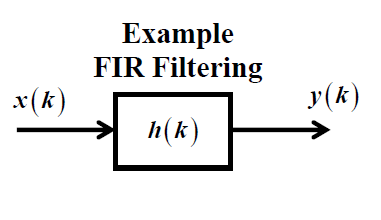
Take an Example of FIR filtering both by a General Purpose Processor as well as DSP


An FIR (Finite Impulse Response filter) is represented as shown in the following figure.
The output of the filter is a linear combination of the present and past values of the input. It has several advantages such as:
- Linear Phase.
- Stability.
- Improved Computational Time.

information shared by www.irvs.info
Subscribe to:
Posts (Atom)